DThe eyes of AI: How mSEMs map the nano-world.
At NanoWorldMaps, advanced imaging technologies such as multi-beam scanning electron microscopes (mSEMs) are more than just microscopes – they act as the sensory organs of artificial intelligence. These instruments generate nanometer-precise data sets on a petabyte scale and enable AI to not only analyze the complexity of the physical world, but to perceive it.
Whether mapping neuronal connections in neuroscience, discovering hidden structures in high-performance materials or inspecting complex semiconductor architectures – high-resolution imaging forms the basis for next-generation scientific findings.
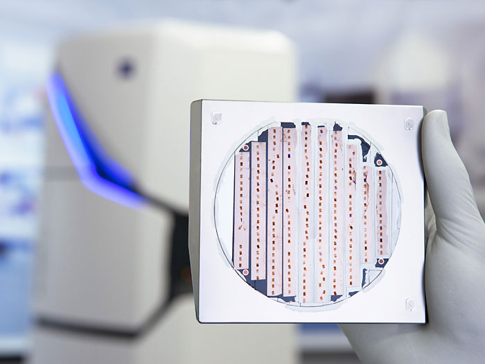
The mSEM uses 91 electron beams working in parallel, enabling ultra-fast, high-resolution imaging of even macroscopic objects on a nanometer scale. The technology is ideal for analyzing semiconductor chips, nanomachines, biological tissue samples or complex organ structures such as the brain. From 2025, NanoWorldMaps will provide access to electron microscopic examinations with the MultiSEM (mSEM) from Zeiss Microscopy.
About NanoWorldMaps
Europe’s new research infrastructure for ultrafast 2D/3D imaging
NanoWorldMaps is a planned, Europe-wide distributed research infrastructure that will provide scientists from industry and research with access to state-of-the-art technologies for ultrafast and large-scale 2D/3D imaging at the nanometer scale. The aim is to position Europe as a leader in high-throughput, multimodal imaging on the nanometer scale.
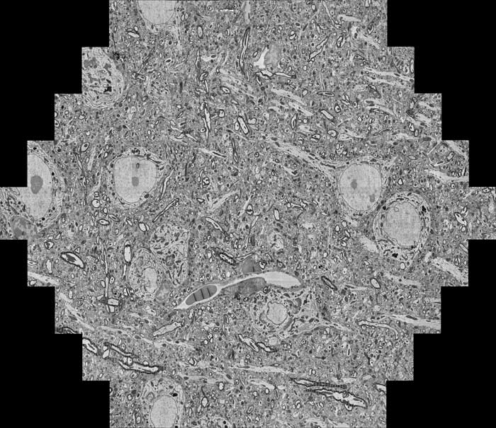
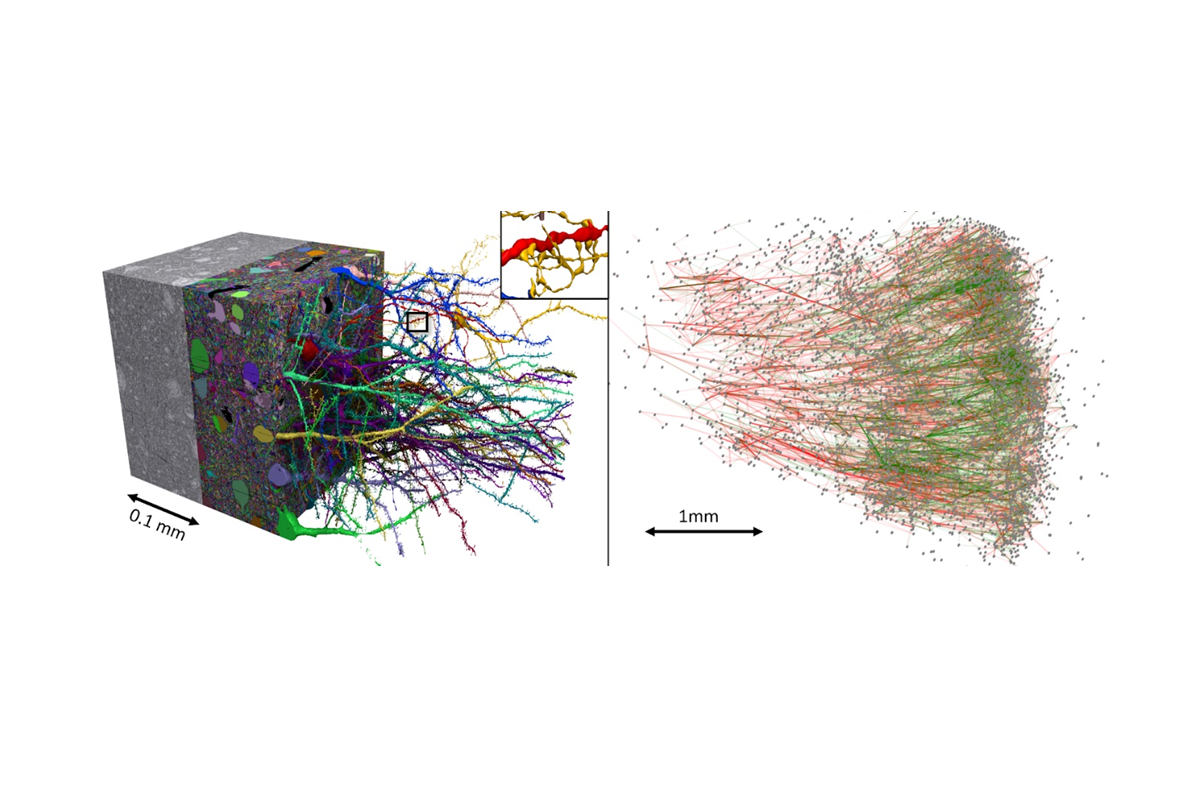
multi-beam_mouse-brain
multi beam image of mouse brain
Core technologies:
Fields of application:
Access and services:
NanoWorldMaps is currently in the concept phase and is working on an integrated service concept that ranges from sample preparation and image acquisition to data analysis using supercomputers and artificial intelligence. The provision of validated data on various scientific cloud systems is also planned.
Further information can be found on the official website: https://nanoworldmaps.eu


